基于DE1-SOC的My_first_fpga
1. 双击桌面的Quartus图标打开Quartus工具。
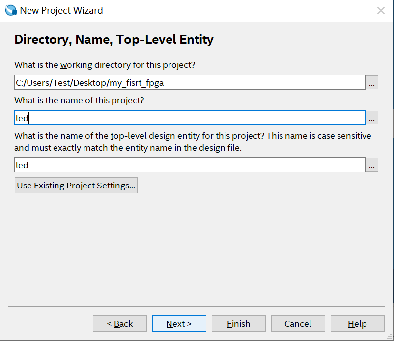
2. 指定工程路径。
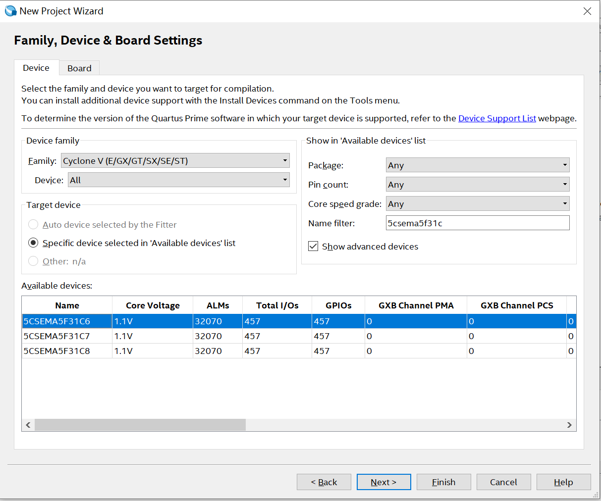
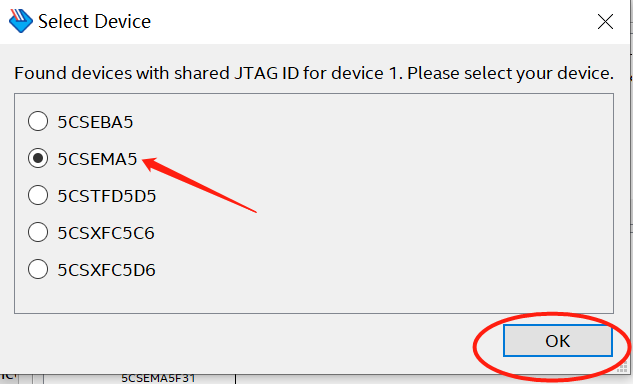
3. 点击四次Next,选择5csema5f31c6器件(这个器件正好是DE1-SOC开发板上对应的FPGA device):
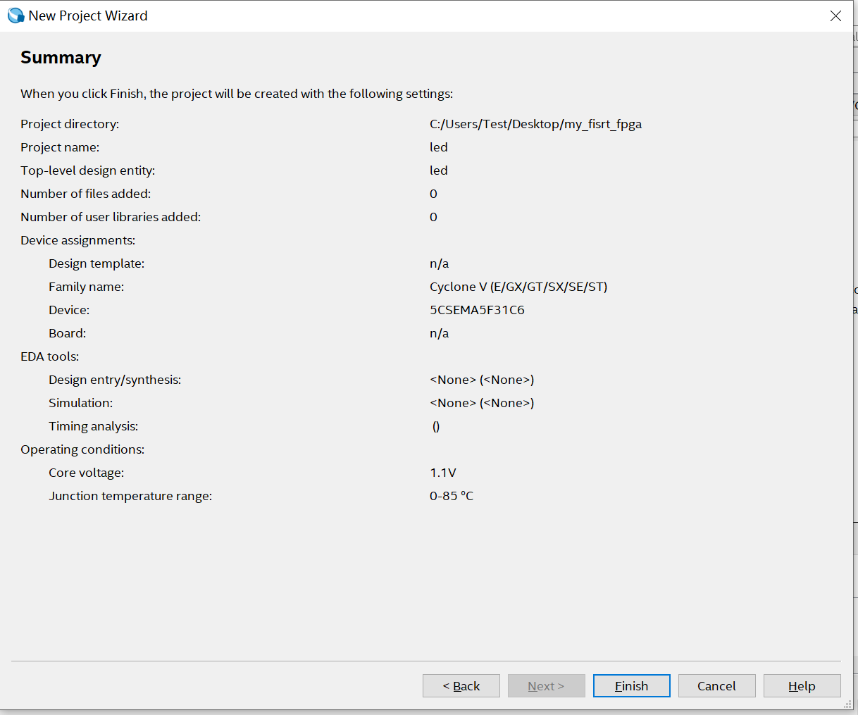
4. 再点击三次Next,然后点击Finish,这样工程就创建好了。
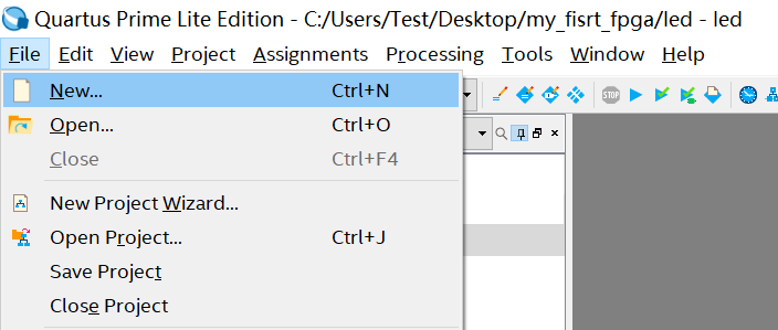
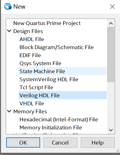
5. 点击File——New,选择Verilog HDL File,点击OK来创建top文件。
6. 将点亮LED 的verilog代码复制到.v文件当中:
module led(
input wire clk, // 50MHz input clock
output wire LED // LED ouput
);
// create a binary counter
reg [31:0] cnt; // 32-bit counter
initial begin
cnt <= 32'h00000000; // start at zero
end
always @(posedge clk) begin
cnt <= cnt + 1; // count up
end
//assign LED to 25th bit of the counter to blink the LED at a few Hz
assign LED = cnt[24];
endmodule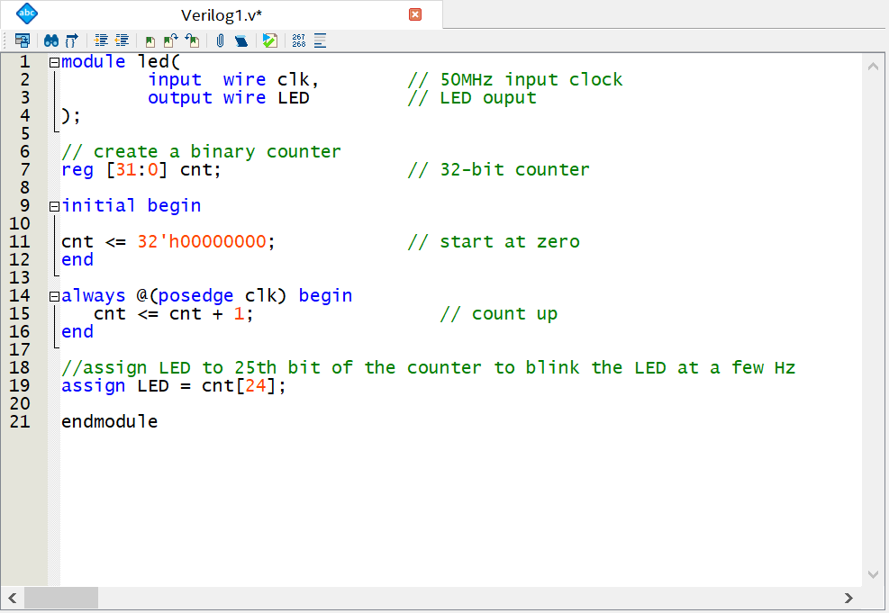
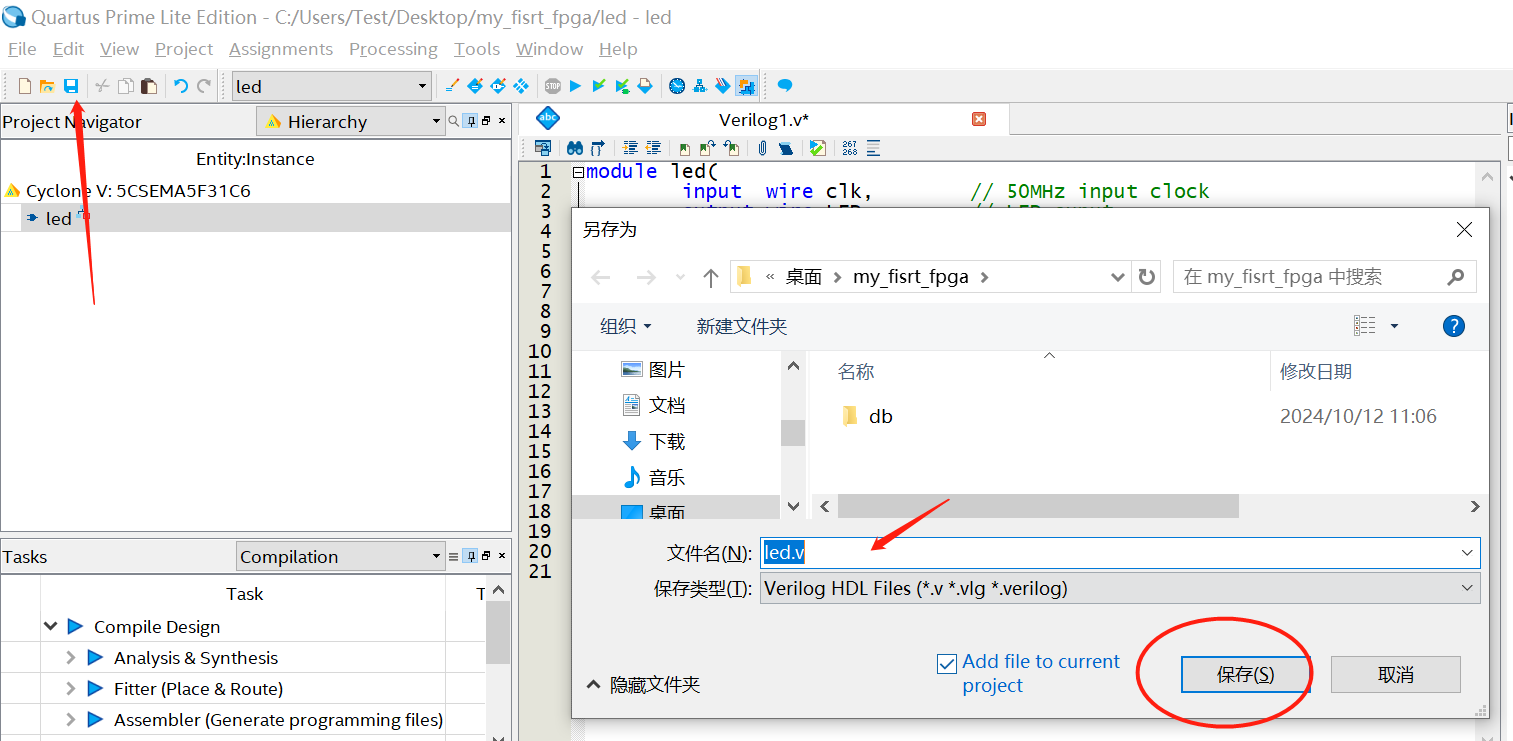
7. 点击保存:
8. 点击分析与综合:
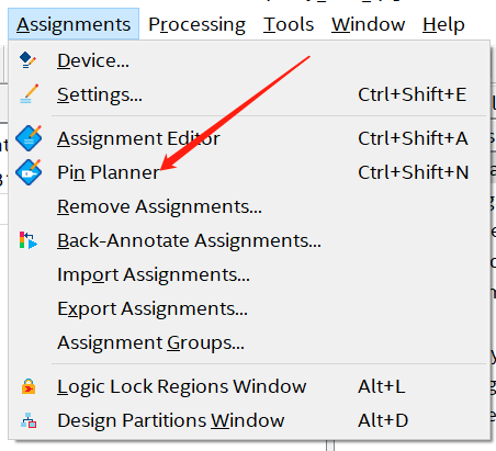
9. 点击Pin Planner:
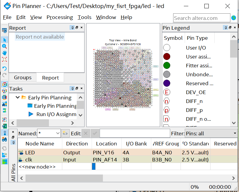
10. 引脚分配如下:
11. 关闭Pin Planner窗口,进行全编译:
12. 给DE1-SOC开发板上电,插上USB Blaster线缆并连接到PC机。
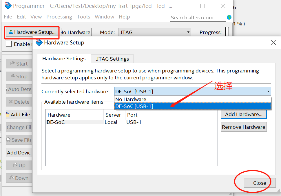
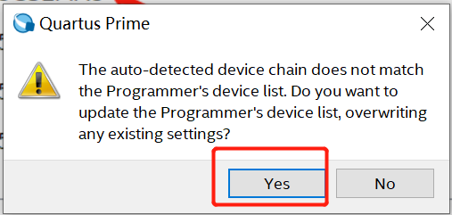
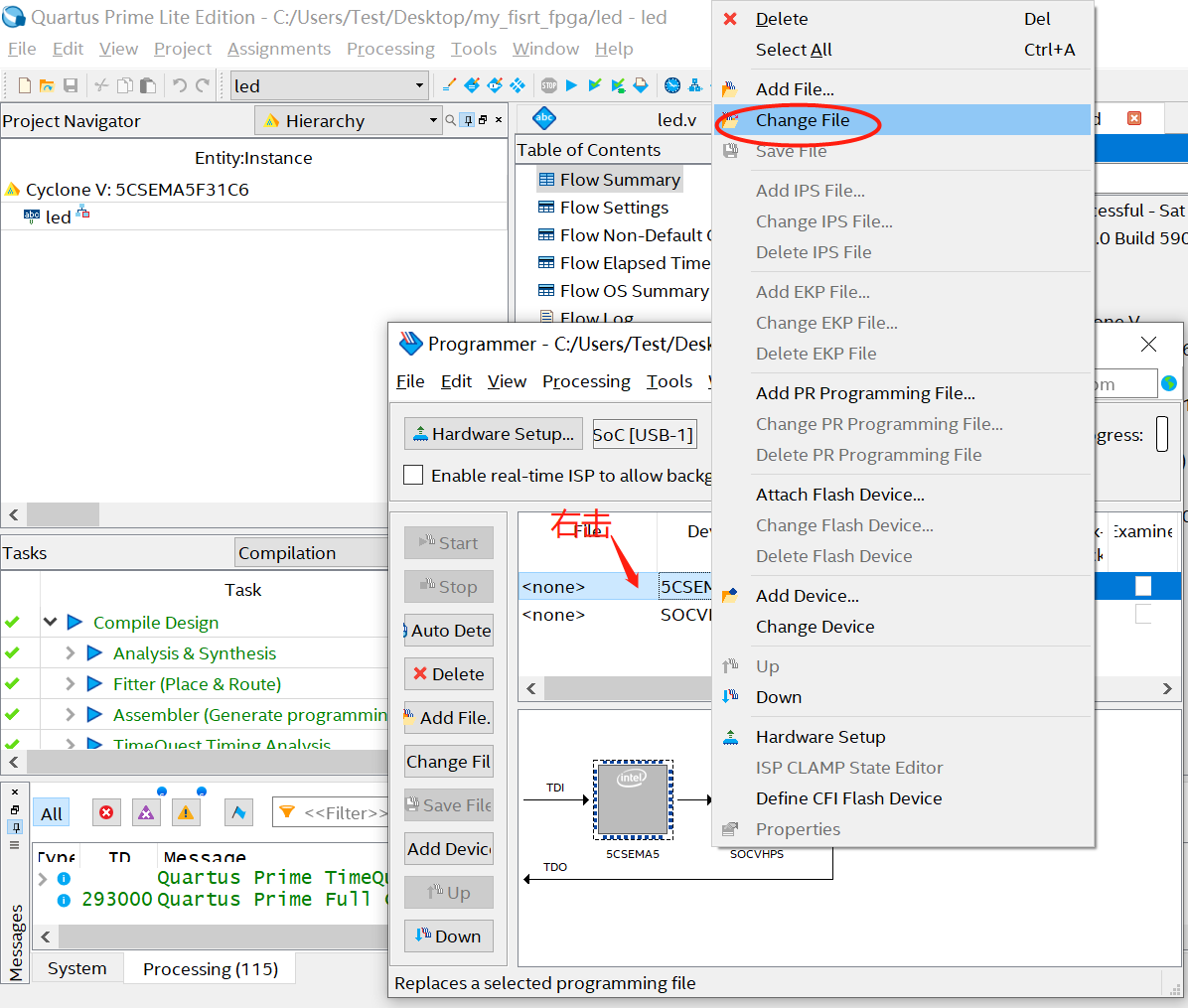
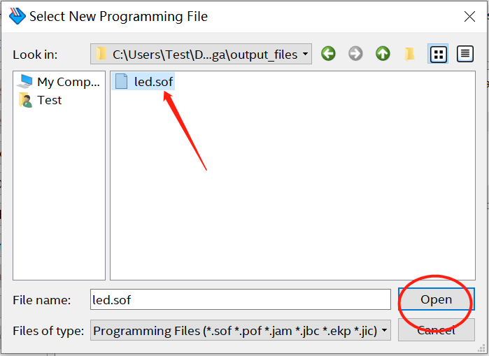
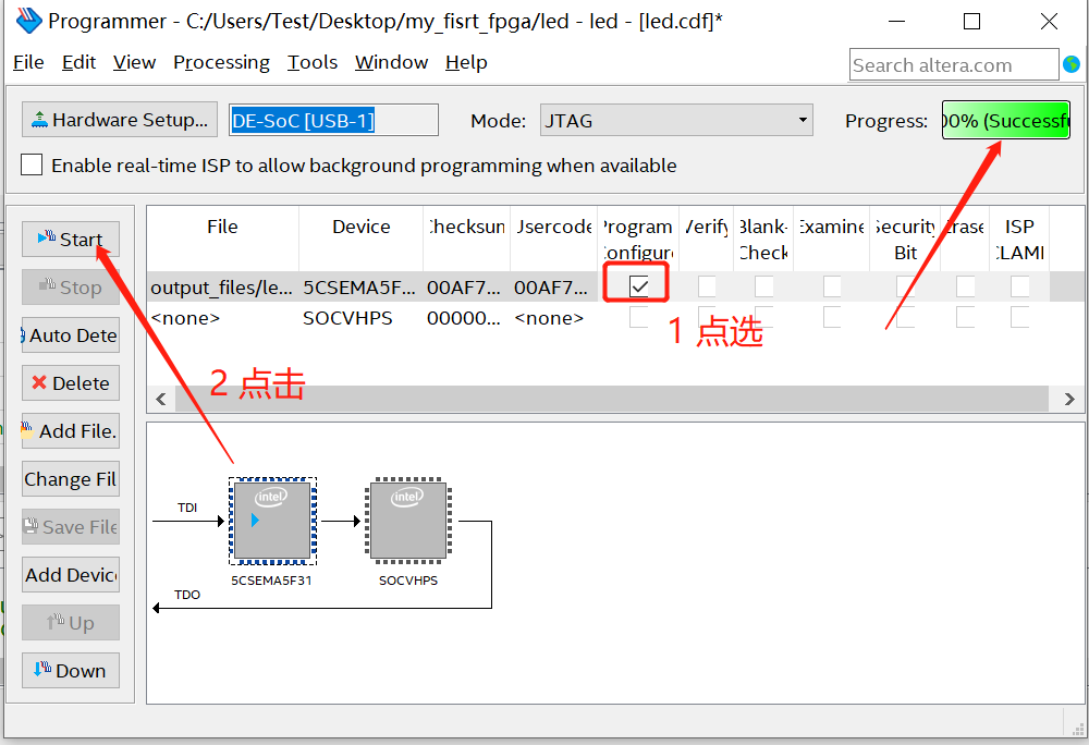
13. 打开Programmer窗口进行sof文件的下载:


可以观察到DE1-SOC的LEDR0在闪烁:

原文地址:https://blog.csdn.net/weixin_47841246/article/details/142876736
免责声明:本站文章内容转载自网络资源,如本站内容侵犯了原著者的合法权益,可联系本站删除。更多内容请关注自学内容网(zxcms.com)!